I’m currently working on a PCB for an 8x8x8 LED cube. The PCB layout in the current status you can find below:
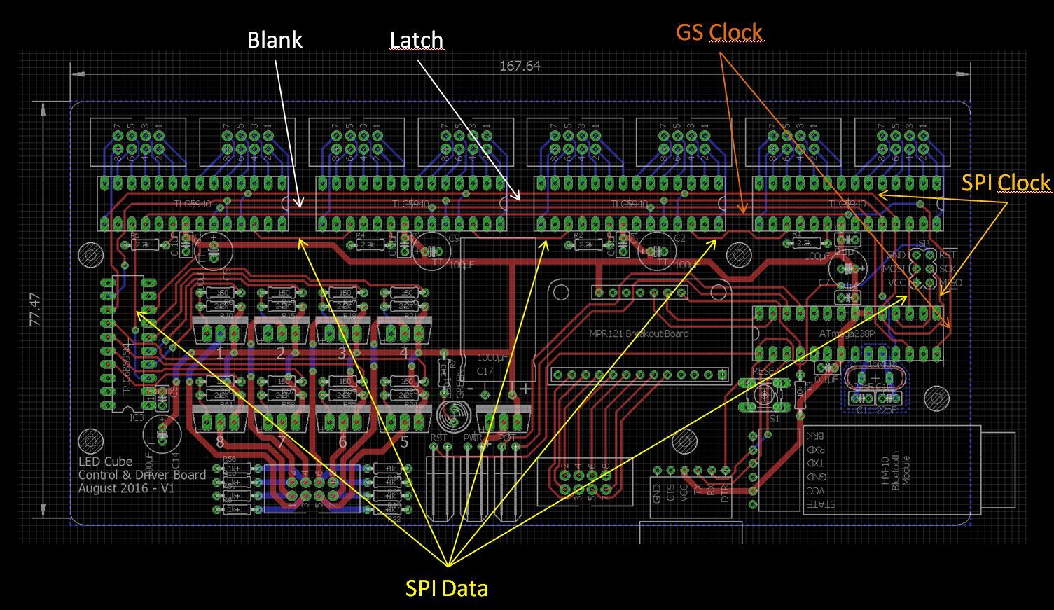
The ATmega328P (16Mhz) will use SPI to send the needed data to four TLC5940 chips (12bit grey scale, 16 channel LED driver) and one TPIC6B595 (8 bit shift register). In order to get high enough FPS and still have enough CPU time for effects the SPI interface needs to run at 8 MHz.
I’m a little bit unsure about the correct layout to avoid problems like corrupted data.
Relevant layout parts for this questions:
A) SPI Data: From the ATmega SPI pin to the first TLC and then daisy chained via the next three TLCs to the TPIC (every trace ~2-3cm long)
B) SPI Clock: From the ATmega SPI Clock pin in two directions. Firstly to the corresponding ISP header and secondly under all the TLCs to the TPIC. Every TLC data clock pin is connected by a very short branch of the clock line. The line ends in the clock pin of the TPIC chip. (total line length ~23-25cm long without branches)
C) GS Clock: Needed to keep the grey scale PWM of the TLCs going. Via the set CKOUT fuse a constant 8Mhz signal is send via this line to all TLC greyscale clock pins (~20cm long without branches).
D) Blank: From ATmega to all TLCs, ending in the last one. Usually GND level, toggled regularly to reset PWM counter in TLCs. During data update for the TLCs it is high for the first few transmitted bytes and then set low again while the rest of the bytes is shifted out (to reduce LED downtime)
E) Latch: From ATmega connected to all TLCs and the TPIC chip. Always low except for a quick toggle (when SPI is not active)
F) PCB Layers: Red lines top, blue lines bottom. The bottom has additionally a complete ground fill, as seen in the magnification of one TLC:

My questions regarding the data transmission layout:
1) Is it ok to route those lines over ~14cm in parallel? Blank und latch (“calm lines”) are in the middle and the “noisy” lines GS Clock and SPI clock on the outside (0.05 inch distance between each line), but therefore close to IC pins.
2) Are the short 90° branches ok to connect every IC to the data lines or will this create problems?
3) What about signal reflection/termination (for SPI and GS clock)? I’ve read several articles about that topic but did not really understand all of it. Some people claim that at 8Mhz there is no problem. Others differentiate between trance length and so on. Some solutions like end line termination apparently are only working for a single load, therefore this will not work for me obviously. So far I haven’t found anything concrete/clear regarding this topic. I feel like this could be a dealbreaker for my board at the moment.
4) What about the signal return path? I tried to make it possible for the return current to follow the relevant top trace on the bottom layer, but a few obstacles remain (like the connections of the GS clock, latch and blank traces to the PLC pins). Is the layout in this respect still ok?
Best regards,